ESP32-S3 Robotics Controller Hub
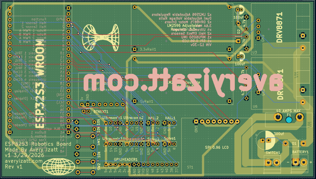
One of the biggest milestones in my recent work has been designing my first fully custom PCB: a 4-layer, ESP32-S3 based robotics controller hub. This board was built to consolidate the many separate modules, wiring harnesses, and prototype systems I had been using into a single, clean, and scalable platform for robotics development.
Design Overview
At the core of the system is the ESP32-S3, chosen for its processing capability, flexible GPIO matrix, integrated WiFi and Bluetooth, and strong support for real-time control tasks. Around it, I designed a complete control and sensing ecosystem intended for mobile robotics applications.
The board integrates:
- Dual DRV8871 motor drivers for bidirectional DC motor control
- Support for two servo outputs with PWM control
- Four ultrasonic sensor interfaces for environmental awareness
- Two hall effect sensor inputs for feedback such as wheel speed or position tracking
- A SPI-connected display for onboard telemetry, debugging, and UI
- Onboard linear regulation and power distribution
- Expansion headers for unused GPIO to support future features
The goal was not just to “make it work,” but to build something robust, reusable, and electrically sound.
Moving from Wiring to PCB Design
Prior to this board, most of my systems were built using breadboards or modular components. While flexible, those setups quickly became unreliable and difficult to maintain, especially when dealing with motors and multiple sensors. This project was my transition into designing a dedicated hardware platform.
The schematic design phase was relatively straightforward. The real learning curve came during PCB layout.
4-Layer Stackup and Grounding Strategy
This board uses a 4-layer stackup, which allowed for a much more controlled and professional layout compared to a 2-layer design. The layers were organized as:
- Top Layer: signal routing and high-current paths
- Inner Layer 1: solid ground plane
- Inner Layer 2: power distribution (VM and regulated rails)
- Bottom Layer: additional signal routing and localized pours
A continuous ground plane was one of the most important design decisions. Instead of routing ground as traces, I used large copper pours and stitching vias to create a low-impedance return path across the entire board. This significantly improves noise performance and reduces the likelihood of instability, especially with switching motor loads.
High-Current Design Considerations
Driving motors introduces large and rapidly changing currents, which can easily create voltage drops, EMI, and system instability if not handled properly.
To address this:
- High-current paths were routed using wide copper traces and local pours
- Motor driver ground connections were reinforced with multiple stitching vias into the ground plane
- VM (motor supply voltage) was kept as a controlled, localized copper region rather than a full-plane pour
- Return paths were kept as short and direct as possible to minimize loop area
One key concept I learned was that current does not just follow the forward path, it follows a loop. Designing tight, low-impedance loops between VM and GND was critical for stable operation.
Decoupling and Noise Reduction
Decoupling capacitors were placed strategically throughout the board, particularly:
- Close to the ESP32-S3 power pins
- Adjacent to each motor driver
- Between VM and ground near high-current switching areas
Both bulk capacitors and small ceramic capacitors were used to handle different frequency ranges of noise. Placement was just as important as value. Keeping these components physically close to the devices they support dramatically improves effectiveness.
Signal Integrity and Peripheral Integration
With a mix of analog-like signals (ultrasonic sensors), digital inputs (hall sensors, buttons), PWM outputs (servos), and high-speed communication (SPI display, I2C IMU), careful routing was required.
Key considerations included:
- Keeping noisy motor and power traces away from sensitive sensor lines
- Using short, direct routes for SPI signals to the display
- Maintaining clean pull-up configurations for I2C communication
- Ensuring proper voltage compatibility, particularly for ultrasonic sensor echo lines
Expandability and Practical Design
A portion of the design was dedicated to future-proofing. Unused GPIO pins were broken out into a dedicated header along with power and ground, allowing additional modules or features to be added without redesigning the board.
This was a deliberate choice to make the board not just a one-off project, but a reusable platform.
What I Learned
This project reinforced that PCB design is not just about making electrical connections, it is about managing current flow, noise, and physical layout in a way that supports reliable operation.
Some of the biggest takeaways:
- Grounding strategy is critical and should be planned early
- High-current paths must be treated differently than signal traces
- Component placement often matters more than routing
- Decoupling and return paths directly affect system stability
- Planning for expansion saves time in future iterations
Looking Forward
This board represents a major step forward in both my electronics design and system integration skills. It replaces a complex, error-prone wiring setup with a compact, reliable controller that can serve as the foundation for future robotics projects.
The next phase will involve assembling, testing, and iterating on the design. I expect there will be improvements to make, but that is part of the process.
Designing this board has been one of the most rewarding technical challenges I’ve taken on so far, and it sets the stage for more advanced and refined hardware in the future!
How to Use the Robotics Controller
This controller is designed to act as a central hub for motor control, sensing, and user interaction. The system is built around the ESP32-S3 and uses a mix of PWM, digital I/O, I2C, and SPI peripherals.
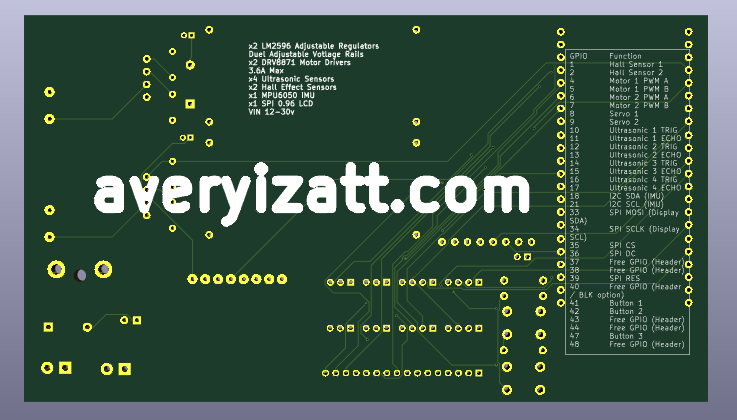
GPIO Pin Reference
GPIO | Function
1 | Hall Sensor 1
2 | Hall Sensor 2
4 | Motor 1 PWM A
5 | Motor 1 PWM B
6 | Motor 2 PWM A
7 | Motor 2 PWM B
8 | Servo 1
9 | Servo 2
10 | Ultrasonic 1 TRIG
11 | Ultrasonic 1 ECHO
12 | Ultrasonic 2 TRIG
13 | Ultrasonic 2 ECHO
14 | Ultrasonic 3 TRIG
15 | Ultrasonic 3 ECHO
16 | Ultrasonic 4 TRIG
17 | Ultrasonic 4 ECHO
18 | I2C SDA (IMU)
21 | I2C SCL (IMU)
33 | SPI MOSI (Display SDA)
34 | SPI SCLK (Display SCL)
35 | SPI CS
36 | SPI DC
39 | SPI RES
41 | Button 1
42 | Button 2
47 | Button 3
Additional GPIO (37, 38, 40, 43, 44, 48) are exposed via header for expansion.
Motor Control (DRV8871)
Motor 1: GPIO 4 (PWM A), GPIO 5 (PWM B)
Motor 2: GPIO 6 (PWM A), GPIO 7 (PWM B)
Control:
- PWM A high, PWM B low → forward
- PWM A low, PWM B high → reverse
- Both low → coast
- Both high → brake
Servo Outputs
Servo 1 → GPIO 8
Servo 2 → GPIO 9
Standard 50 Hz PWM:
- ~1.0 ms pulse → 0°
- ~1.5 ms → center
- ~2.0 ms → 180°
Ultrasonic Sensors
TRIG pins: GPIO 10, 12, 14, 16
ECHO pins: GPIO 11, 13, 15, 17
Operation:
- Send 10 µs pulse on TRIG
- Measure pulse width on ECHO
- Convert to distance
Hall Effect Sensors
Hall 1 → GPIO 1
Hall 2 → GPIO 2
Used for:
- Speed measurement
- Rotation counting
- Position feedback
IMU (I2C)
SDA → GPIO 18
SCL → GPIO 21
SPI Display
MOSI (SDA) → GPIO 33
SCLK (SCL) → GPIO 34
CS → GPIO 35
DC → GPIO 36
RES → GPIO 39
Push Buttons
Button 1 → GPIO 41
Button 2 → GPIO 42
Button 3 → GPIO 47
Use:
pinMode(pin, INPUT_PULLUP);
Expansion Header
Available GPIO:
37, 38, 40, 43, 44, 48
Firmware Template